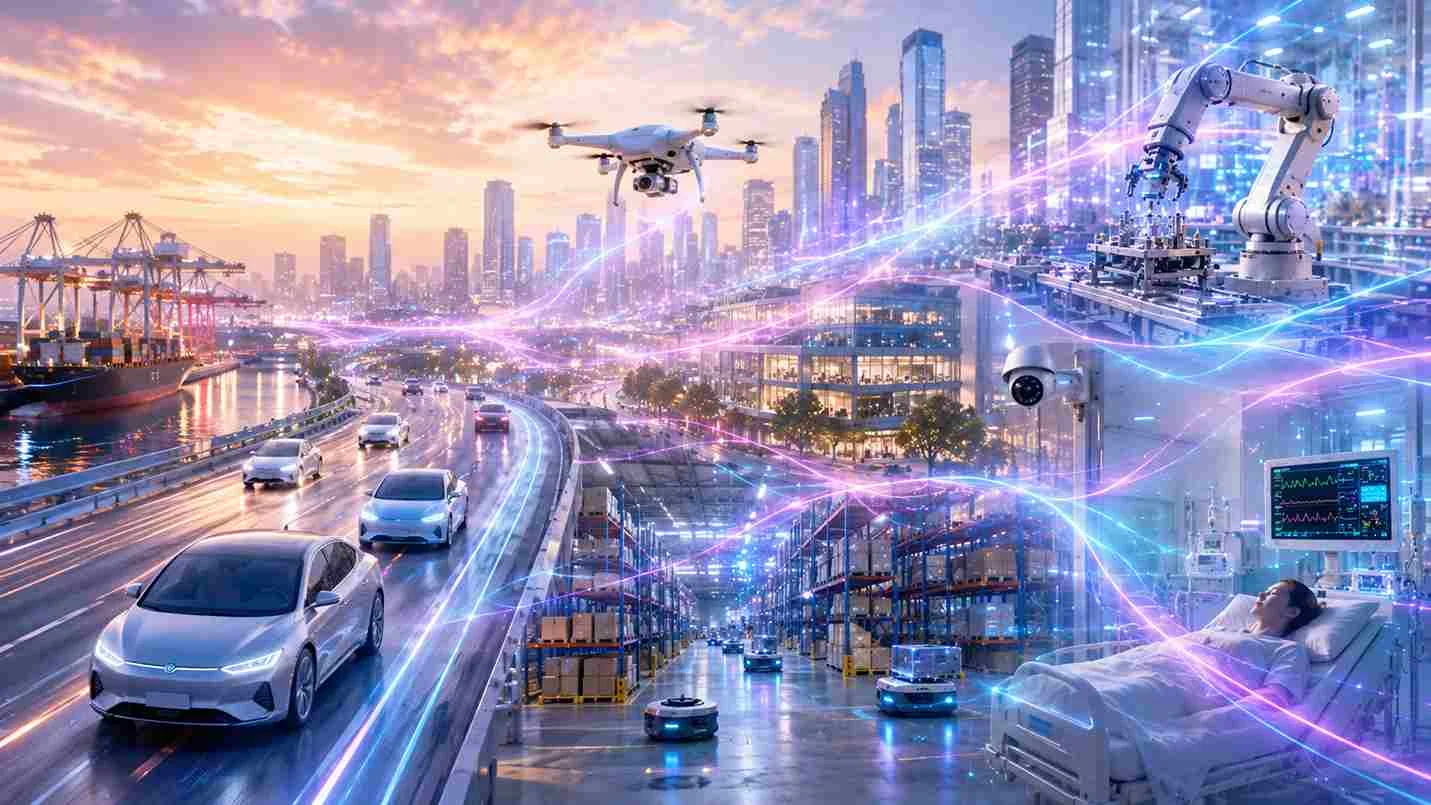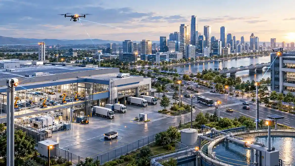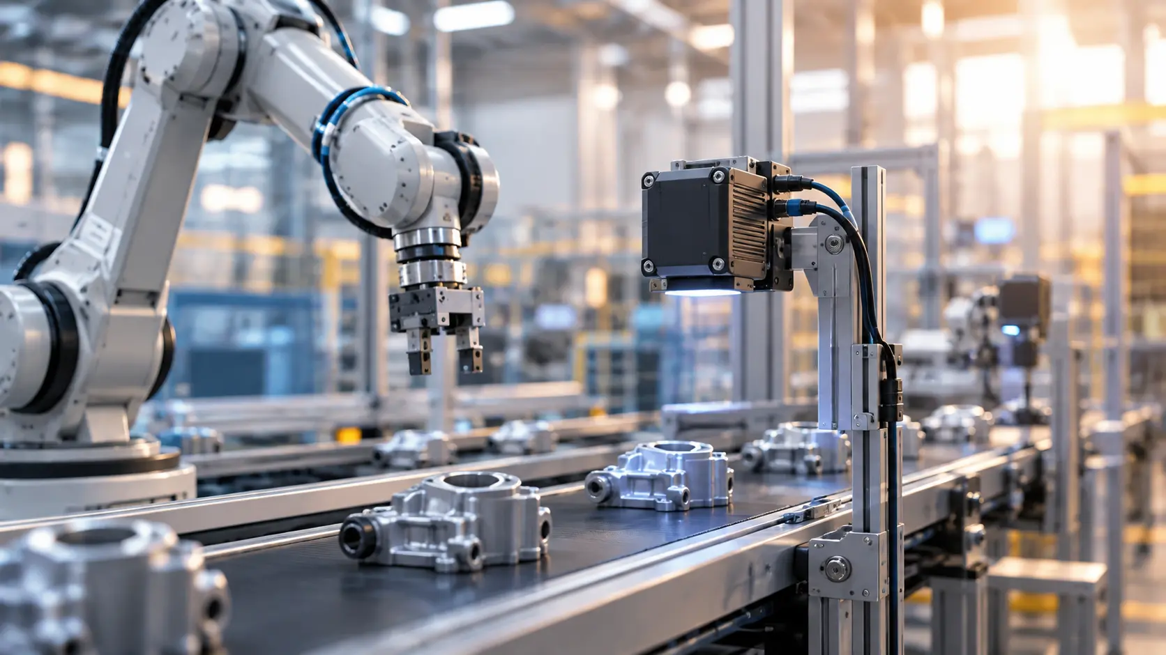

An intelligent vision sensor is an image sensor architecture that embeds computation directly into the pixel array or sensing substrate, so a system extracts task-relevant information at the point of capture instead of streaming full raw frames to a downstream processor for every cycle. The category spans a spectrum, from limited on-chip filtering to fully programmable, software-defined sensing, but the defining trait is the same: processing moves upstream, closer to the photon, to cut the data, power, and latency cost of conventional camera-plus-processor pipelines.
For engineers evaluating machine vision architectures, that shift matters more than any marketing label attached to it. It changes how much silicon, board space, and power budget a design needs to hit a given latency target.
The Data Movement Problem That Drives Sensor Architecture
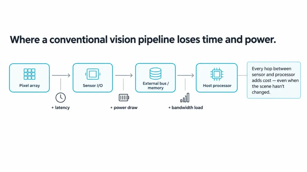
A conventional CMOS image sensor (CIS) has one job: convert incident light into a full-resolution pixel array and push it off-chip, frame after frame, regardless of whether the scene changed. At high frame rates and resolutions, that constant readout becomes the dominant cost in the system, not the compute itself.
Every hop the data takes, from pixel array to sensor I/O, across a bus, into external memory, into a host processor, adds latency and burns power. Partitioning a sensor into separately optimized photodiode and logic wafers, then stacking and interconnecting them, became a mainstream approach precisely because it let each layer be fabricated on the process node best suited to it, reducing cost and die area. That stacked backside-illuminated (BSI) manufacturing approach is now the physical foundation most sensor-level intelligence is built on, including Oculi’s.
The result of ignoring this problem shows up downstream: application processors doing motion detection, tracking, or classification on full video streams spend most of their compute cycles reprocessing redundant, unchanged pixels. For always-on, battery-powered, or bandwidth-constrained systems, that redundancy is the actual engineering constraint, not raw compute capability.
From Frame-Based Capture to Intelligent Vision Sensing
Sensor-level intelligence has developed in stages, and the terms are often used loosely, so it’s worth separating them:
Traditional image sensor– Captures and outputs full frames at a fixed rate; all interpretation happens on a separate CPU, GPU, or NPU.
Edge processing – Interpretation still happens off-sensor, but on compute located physically close to the camera rather than in the cloud.
In-sensor processing – Circuitry within the sensor package performs early operations, such as change detection or basic feature extraction, before data leaves the chip.
In-pixel computing – Processing is embedded at the level of individual pixels or small pixel clusters, so computation happens where the light is actually captured.
Intelligent vision sensing – The pixel array, processing logic, and I/O are unified into a single, typically programmable unit that can be reconfigured for different tasks after deployment.
Each stage reduces how far raw data has to travel before something useful is extracted from it.
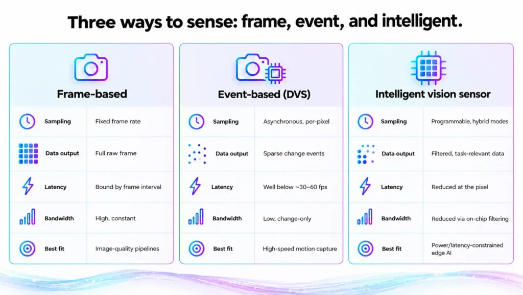
Frame-Based, Event-Based, and Intelligent Vision Sensors Compared
Intelligent vision sensor is sometimes conflated with event-based (neuromorphic) sensors, but they solve the data problem differently.
| Dimension | Frame-based sensor | Event-based (DVS) sensor | Intelligent vision sensor |
| Sampling | Fixed frame rate, every pixel every cycle | Asynchronous, per-pixel response to contrast change | Programmable; frame, event, or hybrid output modes |
| Data output | Full raw frame | Sparse stream of change events with timestamp and polarity | Selectively filtered, task-relevant data |
| Latency | Bound by frame interval | Well below conventional frame rates (typically ~30-60 fps) | Reduced by computing at or near the pixel |
| Bandwidth | High, constant, scene-independent | Low; events produced only on change | Reduced through on-chip data reduction |
| Processing location | External CPU/GPU | Largely external; pixel performs change detection | On-chip, often at the pixel |
| Best fit | Image-quality-driven pipelines | High-speed, high-dynamic-range motion capture | Power, latency, and bandwidth-constrained edge AI |
Event-based sensors solve the redundancy problem by only reporting change; intelligent vision sensors solve it by computing on the data at the source, which is a broader and, for many AI workloads, more directly useful capability, since it can incorporate feature extraction and inference logic rather than raw change signaling alone.
Architecture of an Intelligent Vision Sensor
A typical intelligent vision sensor architecture separates into four functional blocks: a pixel array built from compute-capable pixel units, a readout control block managing how and when data is pulled from that array, an I/O interface to the host system, and an image signal processing stage for any data that still needs conventional formatting.
Each pixel in this kind of array acts not only as a point of light capture but also as an intelligent processor, giving the sensor the ability to selectively capture and process data rather than transmitting a constant, undifferentiated stream. This is architecturally distinct from adding a small co-processor next to a conventional sensor die; the compute is distributed across the array itself.
Processing Approaches and Their Trade-offs
No single architecture wins on every axis, and the trade-offs are what should drive a design decision:
Fixed-function vs. programmable – A sensor hard-wired for one task is simpler and cheaper but can’t be repurposed. A software-defined sensor can be reconfigured post-deployment, at the cost of additional on-chip control logic.
Data reduction vs. information completeness – Aggressive filtering at the pixel reduces bandwidth and power but risks discarding information a downstream algorithm might have needed. The filtering criteria have to match the actual task.
Sparsity vs. throughput– Event-driven and sparse-output modes cut data volume dramatically for scenes with limited motion, but dense, fast-changing scenes can still generate high event rates that erode the bandwidth advantage.
Manufacturing complexity vs. integration density – Stacked, in-pixel architectures require more advanced wafer-bonding processes than a conventional single-layer sensor, which affects yield and cost at scale.
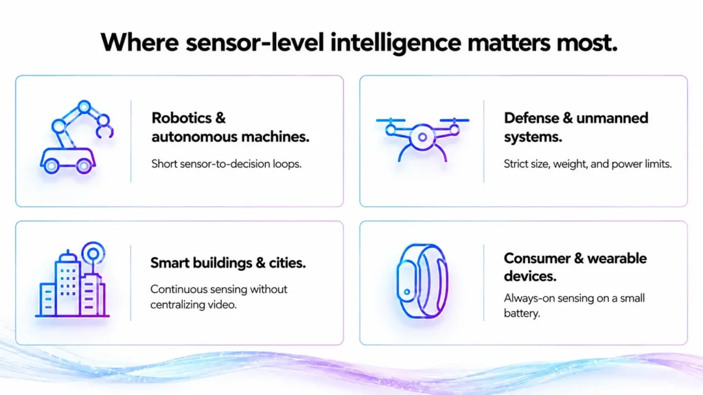
Applications of Intelligent Vision Sensing
The constraints that make sensor-level intelligence valuable, power, latency, bandwidth, and privacy, map directly onto specific classes of deployment:
Robotics and autonomous machines – Obstacle detection and navigation need short sensor-to-decision loops that a full-frame pipeline struggles to sustain at low power.
Defense and unmanned systems – Size, weight, and power (SWaP) budgets often rule out a separate application processor entirely. Oculi has demonstrated its sensor architecture outperforming expensive military imaging systems at 30,000 frames per second with less than 0.3 watts of power consumption.
Smart buildings and smart cities – Occupancy sensing and traffic analytics at scale need to run continuously across many cameras without centralizing raw video, which is as much a bandwidth and privacy problem as a compute one.
Consumer and wearable devices – Always-on gesture, presence, or gaze sensing in AR/VR and IoT hardware depends on sensing that doesn’t drain a small battery.
How Oculi Approaches Intelligent Vision Sensing
Oculi’s SPU (Sensing and Processing Unit) is built around IntelliPixel®, its patented in-pixel computing architecture, where each pixel combines a photodetector, front-end, ALU, and local memory rather than functioning as a passive light-to-charge element. That design is what allows the SPU to be a Software-Defined Vision Sensor™: the same silicon can be reconfigured for different detection tasks, frame-rate profiles, or power envelopes without a new sensor variant.
The OCULI SPU is built to meet the computational demands of machine learning workloads directly on the sensor, rather than optimizing purely for human-viewable image quality, and a partnership with GlobalFoundries supports manufacturing it at scale. For engineering teams evaluating the approach against a specific power, latency, or bandwidth target, Oculi’s Evaluation Programs provide hardware kits and software-only simulators to test the SPU and IntelliPixel® against real application requirements before committing to a design.
For a broader look at how the SPU architecture compares to conventional sensor-plus-processor pipelines, see Oculi’s guide on how the SPU transforms AI vision sensors.
Where Intelligent Vision Sensing Is Headed
As edge AI systems take on more autonomous, real-world decision-making, the industry has started framing this as Physical AI: AI that has to perceive and act in physical space under real power, latency, and mechanical constraints, not just process data in a data center. Intelligent vision sensors are a foundational piece of that shift, since they determine how much of the perception burden a system can carry without a large processor or constant connectivity. Oculi’s markets page outlines how this plays out across smart cities, smart machines, smart devices, and defense platforms. If you’re scoping a design against these constraints, contact us to discuss your application.
Frequently Asked Questions
Is an intelligent vision sensor the same as an AI vision sensor?
They’re closely related AI vision sensor is the broader category, while intelligent vision sensor typically emphasizes deeper, often pixel-level integration of sensing and processing, up to a fully programmable, software-defined architecture.
Do intelligent vision sensors replace event-based (DVS) sensors?
Not necessarily. They address overlapping but distinct problems, sparsity versus computation, and some architectures combine event-driven readout with in-pixel processing.
What manufacturing process do intelligent vision sensors use?
Most rely on stacked, backside-illuminated (BSI) CMOS processes, bonding a sensing layer to a separate logic layer, which leverages the existing CMOS image sensor manufacturing ecosystem rather than a novel process node.
When is a conventional image sensor still the better choice?
When the application is driven primarily by image quality, resolution, or extensive downstream image signal processing, and power or latency aren’t binding constraints.
How programmable are intelligent vision sensors like the OCULI SPU?
Software-defined architectures can be reconfigured for different detection tasks, output modes, and power profiles after deployment, without new silicon.